cetalog-img

Materials for a next-generation (nano-)opto-electro-mechanical systems

Introduction


Today’s information and communication technology (ICT) is essentially governed by information processing using (i) CMOS microelectronics and (ii) distribution of information via optical telecom network.Introducing a third variable – phonons – will lead to additional degrees of freedom in ICT applications.

Exploiting the interaction between the three particles, electrons, photons and phonons, and the available degrees of freedom in the nano-opto-electro-mechanical systems (NOEMS) will open the possibility to an unprecedented advancement of the potential of low power information processing and transmitting, enabling the realization of the next low-power ICT generation technology.

Figure 1. Schematics of the objectives of MAGNIFIC. The heart of the new technology is the miniaturized NOEMS component based on CMOS compatible nanocrystalline silicon and aluminium nitride, operating at telecom light wavelength and in the GHE microwave frequency range. The device will convert THz and GHz signals to suitable bands for internet and mobile applications with very high power-efficiency.

The telecom networks providing IoT connectivity will require massive use of base stations (BS) or access nodes at the optical network units (ONUS) which will be interconnected via optical fibers. The target frequency range of NOEMS components will be 3-6 GHz and 8-12 GHz for 5G and satellite communication (SATCOM), respectively. NOEMS can operate at such spectral regimes by engineering nanobeams that can be interfaced with telecom-wavelength optics and electronics. The extreme miniaturization, when implemented in silicon integrated circuitry, with mechanical and optical fields overlapping in wavelength-scale regions, results in strong electro-mechanical (EM) and optomechanical (OM) interactions, enabling low-power and efficient devices.

The long-term vision of MAGNIFIC is that current and next generation access networks will include low-cost power-efficient silicon-based NOEMS – combining optical fiber telecom as well as RF electronics – enabling the realization of power efficient network functions such as photonic local oscillators, channel frequency conversion and electro-optical modulation. However, to implement this vision, fundamental scientific, materials properties and fabrication related challenges need to be solved (see box below).

SCIENTIFIC AND TECHNOLOGICAL GOALS

MAGNIFIC will do that by pursuing the following main scientific and technological goals:


To investigate and optimize the properties of nanocrystalline silicon for NOEMS components and optimize piezoelectric coupling with aluminium nitride.


To enhance the electromechanical coupling in NOEMS structures required to reach GHz range in operation using acoustic metasurfaces to manipulate the mechanical energy flow.


To understand the energy flow into and in a mechanical oscillator to control the frequency fluctuations and improve the long-term stability.


To identify the challenges related to fabrication processes, e.g., the effects of variability and tolerances.


To realize a power-efficient demonstrator for 5G and SATCOM applications and establish the first version of the fabrication process for the devices.

THE BUSINESS CASE WILL INCLUDE THE FOLLOWING STEPS:

Market Analysis

Market analysis of the possible applications, in terms of: (a) targeted markets, (b) estimated market size in the EU and globally, (c) end-users needs, (d) market segmentation.

Competitive arena

Analysis of competitive arena, i.e., benchmark with the traditional solutions and products available on the markets.

SWOT analysis

SWOT analysis, i.e., possible risks and market barriers of introducing the developed technologies.

Production costs

Analysis on the production costs of mentioned possible applications.

Use case

Selection of the best use case.

TTM strategy

Definition of the tech-to-market strategy and on the industrialization process.

IMPACT

SPECIFIC NEEDS

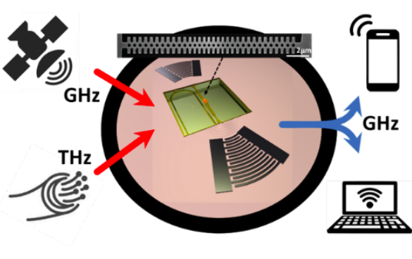
• Massive deployment of ICT devices and networks (5G, IOT) for cost-effective, low power and compact optoelectronic interfaces where RF electronics and optics coexist are needed.

• The selected platform core material, ensuring CMOS – compatible fabrication, is nc-Si due to its electronic, optical, and additional, mechanical properties, which must be understood to design advanced devices and circuits.

EXPECTED RESULTS

• Publication of a review paper on optical, mechanical, thermal, and electronic properties of nc-Si, with theoretical and experimental results, in a major scientific journal.

• Models of dynamic properties of nc-Si suitable for NOEMS.

• Database on properties of nc-Si

• Understanding and control of fluctuations and noise in NOEMS to improve platform.

D & E & C MEASURES

Dissemination towards the scientific community and industry: Publishing scientific results in major journals in photonics, physics, and nanotechnology; participating in specialist conferences, at EC project portfolio and at relevant industry events (Photonics21, KDT JU) to disseminate the results as part of a group and maximise the visibility vis-à-vis companies. Arranging meetings with selected industrial stakeholders.

Exploitation of the new product: We plan to patent the technology of nc-Si nanomechanical oscillators and of the new platform to process optically RF data in two frequency ranges.

Communication: Creation of a Website and Twitter account. News releases and e-Newsletters. Creation of a video explaining our technology once IP has been protected. Link project via LinkedIn to EU Digital Europe, to the JU KDT and Photonic21. Send e-Newsletter to national/regional photonics and KDT mirror industrial associations.

This project has received funding from the European Union’s Horizon Europe research and innovation programme under grant agreement No 101091968.


The sole responsibility for the content of this webpage lies with the authors. It does not necessarily reflect the opinion of the European Union.
Neither the REA nor the European Commission are responsible for any use that may be made of the information contained therein.

Get In Touch

Write to us

Principal Investigator contact:

Marco Miniaci

    This project has received funding from the European Union’s Horizon Europe research and innovation programme under grant agreement No 101091968. The sole responsibility for the content of this webpage lies with the authors. It does not necessarily reflect the opinion of the European Union. Neither the REA nor the European Commission are responsible for any use that may be made of the information contained therein.